(China (Mainland))


Product Summary
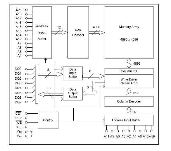
The BS62LV1600EIP55 is a high performance, very low power CMOS Static Random Access Memory organized as 2048K by 8 bits and operates form a wide range of 2.4V to 5.5V supply voltage. Advanced CMOS technology and circuit techniques provide both high speed and low power features with typical CMOS standby current of 1.5μA at 3.0V/25O℃ and maximum access time of 55ns at 3.0V/85OC. Easy memory expansion is provided by an active LOW chip enable (CE1), an active HIGH chip enable (CE2), and active LOW output enable (OE) and three-state output drivers. The BS62LV1600EIP55 has an automatic power down feature, reducing the power consumption significantly when chip is deselected. The BS62LV1600EIP55 is available in JEDEC standard 44-pin TSOP II and 48-ball BGA package.
Parametrics
BS62LV1600EIP55 absolute maximum ratings: 1)VTERM Terminal Voltage with Respect to GND: -0.5V to 7.0 V; (2)TBIAS Temperature Under Bias: -40℃ to +125℃; (3)TSTG Storage Temperature: -60℃ to +150℃; (4)PT Power Dissipation: 1.0W; (5)IOUT DC Output Current: 20mA.
Features
BS62LV1600EIP55 features: (1)Wide VCC operation voltage: 2.4V to 5.5V; (2)Very low power consumption: VCC = 3.0V Operation current : 46mA (Max.) at 55ns, 2mA (Max.) at 1MHz; Standby current : 1.5uA (Typ.) at 25℃; (3)VCC = 5.0V Operation current : 115mA (Max.) at 55ns 10mA (Max.) at 1MHz; Standby current : 6.0uA (Typ.) at 25℃; (4)High speed access time: 55 55ns (Max.) at VCC : 3.0 to 5.5V; 70 70ns (Max.) at VCC : 2.7V to 5.5V; (5)Automatic power down when chip is deselected; (6)Easy expansion with CE1, CE2 and OE options; (7)Three state outputs and TTL compatible; (8)Fully static operation; (9)Data retention supply voltage as low as 1.5V.
Diagrams